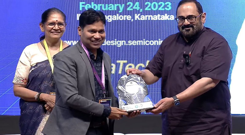
The Minister of State for Electronics & Information Technology and Skill Development & Entrepreneurship, Shri Rajeev Chandrasekhar today launched the 2nd Semicon India FutureDESIGN Roadshow at IISc in Bengaluru with an aim to encourage startups, next-generation innovators, and business leaders to invest in semiconductor sector in India.
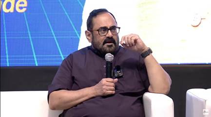
MoS Shri Rajeev Chandrasekhar addressing at 2nd Semicon India FutureDESIGN Roadshow
Speaking on the occasion, Shri Rajeev Chandrasekhar said India is growing rapidly in global electronics value chains and rapid growth of digitalization, along with India’s high-growth digital and innovation economy, has created opportunities in the New World Order of Semiconductor and Electronics.
He spoke about three trends that are currently visible, “First, there has been an acceleration in digitalisation and governments around the world are digitising rapidly. Secondly, we are at an inflection point, and third, for the world, New India is becoming a trusted partner in terms of delivering talent, global products, digital products and services.”
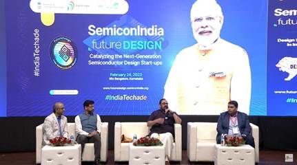
MoS Shri Rajeev Chandrasekhar addressing at 2nd Semicon India FutureDESIGN Roadshow
Emphasising that the Prime Minister Shri Narendra Modi is relentlessly working for expanding opportunities for Young Indians he said Semicon India FutureDESIGN represents one such opportunity.
Outlining some of the initiatives that the Government has taken to support the semiconductor innovation ecosystem in India, Shri Rajeev Chandrasekhar said that the India Semiconductor Research Centre (ISRC) which will be a private, industry led research centre will soon be launched and the Semiconductor Laboratory is being modernised and pivoted into research fab and will be co-located with the ISRC.
In addition, the Government plans to introduce an educational curriculum as part of the Future Skills programme, he said. “It has been developed in collaboration with industry experts and academics. A large number of colleges will have new degrees, new electives, and new certification programs in VLSI. We are actively working with fab companies to create on the job training type of internships for students in the semiconductor space,” he stressed.
The Minister also announced the launch of the ChipIN Centre at C-DAC India, Bangalore which will act as one stop centre to provide Semiconductor Design Tools, Fab access, Virtual Prototyping Hw Lab access to Fabless Chip Designers of the country. He also said that India AI Datasets program is going to be launched soon. It will be the world’s largest datasets program which will in turn catalyse the Intelligent compute, AI compute, device and the system design ecosystem, he added.
Speaking about the potential for collaboration between Indian startups and Global semiconductor majors, he stated that Global Semicon majors can enhance their ability to innovate beyond the normal innovation horizon through the power of SemiconIndia FutureDESIGN Startups.
Shri Rajeev Chandrasekhar outlined India’s ambitions with respect to the DIR-V (Digital India RISC-V Microprocessor Program) which will help develop, siliconize and create design wins for future around SHAKTI and VEGA RISC-V Processors and commercial grade Indian Processors this year. “We are building a comprehensive architecture around RISC-V and aims to make India a RISC-V Talent hub for the world,” he said.
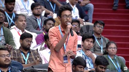
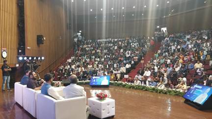
The Minister’s address was followed by an interactive session with members of the audience.
Shri Rajeev Chandrasekhar announced the first set of startups selected under the Semicon India Future Design DLI scheme. The startups are Vervesemi Microelectronics Pvt. Ltd, Fermionic Design Pvt. Ltd. and DV2JS Innovation Ltd. The CEOs of these startups had interactions with several industry leaders including Dr Sailesh Chittipeddi, President, GM and Board member Renesas Electronics and Mr Anand Ramamoorthy, MD, Micron Technology India.
The Scheme aims to offer financial incentives as well as design infrastructure support across various stages of development and deployment of semiconductor design(s) for Integrated Circuits (ICs), Chipsets, System on Chips (SoCs), Systems & IP Cores and semiconductor linked design(s) over a period of five years.


