Odisha Signs Landmark Semiconductor Manufacturing Agreement
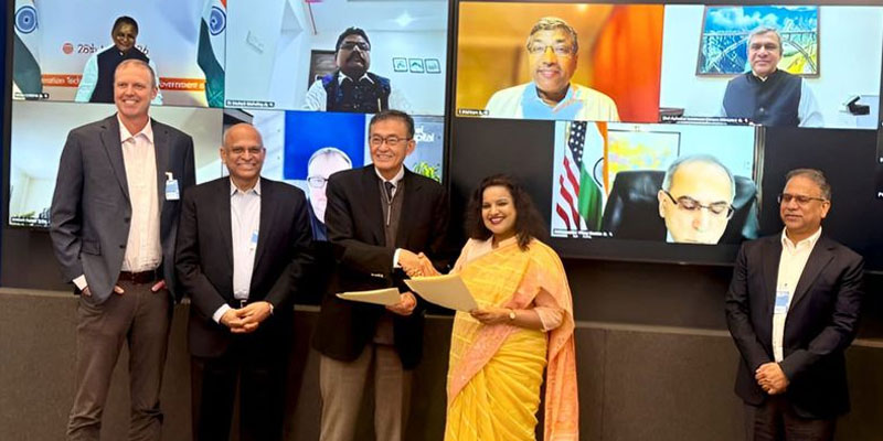
The Odisha government has signed a significant Memorandum of Understanding (MoU) with Intel and 3D Glass Solutions (3DGS) to bring advanced semiconductor substrate manufacturing technology to India. Announced by Union Electronics and Information Technology Minister Ashwini Vaishnaw, the agreement marks a major milestone in India’s efforts to build a robust domestic semiconductor ecosystem and reduce reliance on imported chip technologies.
India’s Drive for Semiconductor Self-Reliance
Over the past few years, India has intensified efforts to establish itself as a key player in the global semiconductor industry. The government’s Semicon India Programme has sought to attract investments across chip manufacturing, packaging, display fabrication and semiconductor design through a combination of policy support and financial incentives.
Semiconductors have become central to modern economies, powering everything from smartphones and data centres to defence systems and electric vehicles. As global supply chains face increasing geopolitical and economic uncertainties, countries are seeking to localize critical semiconductor capabilities.
Against this backdrop, Odisha has emerged as a strategic destination for semiconductor investments. The latest partnership strengthens the state’s position in a sector viewed as crucial for India’s technological and industrial future.
India’s First Advanced 3D Packaging Initiative
The MoU paves the way for establishing India’s first advanced 3D glass substrate packaging facility in Bhubaneswar’s Info Valley, located in Khordha district. The project will be developed by US-based 3DGS through its Indian subsidiary and is expected to attract investments of nearly ₹2,000 crore.
The facility will focus on heterogeneous integration packaging, a sophisticated technology that enables multiple semiconductor components to be combined into highly efficient systems. The plant is expected to manufacture around 70,000 glass panels annually while producing nearly 50 million assembled units.
These advanced packaging solutions are expected to serve high-growth sectors such as artificial intelligence, telecommunications, defence, aerospace and next-generation wireless technologies including 5G and 6G.
Commercial production is targeted to begin by August 2028, with full-scale manufacturing anticipated by 2030.
Odisha’s Growing Strategic Importance
The project gives Odisha a unique distinction within India’s semiconductor landscape. The state is set to host both a compound semiconductor fabrication facility and an advanced packaging unit, making it the only state currently positioned across multiple critical segments of the semiconductor value chain.
The participation of Intel adds further significance to the initiative. The collaboration is expected to enhance technology transfer, strengthen industrial capabilities and integrate India more deeply into global semiconductor supply networks.
The development also complements the broader progress of the Semicon India Programme, under which multiple fabrication, packaging and chip-design projects have already received approval across several states.
Building the Foundation for a High-Tech Future
The Intel-3DGS partnership represents more than a new industrial investment; it signals India’s growing ambitions in one of the world’s most strategically important industries. By attracting advanced semiconductor manufacturing and packaging capabilities, Odisha is positioning itself as a vital hub in the country’s technology ecosystem. If executed successfully, the project could generate high-skilled employment, attract further investments and strengthen India’s quest for semiconductor self-reliance, helping the country secure a stronger role in the global electronics and chip supply chain.
(With agency inputs)